
When Semiconductor Fabrication Plants Decision-Makers Need Strategic Presentations Addressing Business Outcomes
Semiconductor Fabrication Plants Presentation Design provides specialized slide deck structuring, visual technical translation, and graphic design for executive reviews, investor proposals, and operational updates across the microelectronics manufacturing sector.
Presentation Gurus provides specialized slide deck production engineered for executives in semiconductor manufacturing. Capital expenditure requests, process node yield reports, and CHIPS Act funding proposals demand rigorous narrative precision. Engineering leadership cannot afford misaligned visual structures when presenting multi-billion-dollar cleanroom expansions to institutional investors or government agencies. We design technical PowerPoint collateral and investor pitch deck assets that translate complex yield curves, lithography requirements, and wafer capacity metrics into clear commercial drivers.
Why Semiconductor Fabrication Plants Presentations Need Professional Presentation Design
Semiconductor Fabrication Plants operate under severe capital intensity and lengthy return horizons. Generic presentation decks fail to communicate the complex operational dependencies of cleanroom throughput, sub-3nm process yields, and supply chain bottlenecks. Decision-makers tuned to capital efficiency discard vague visual metaphors and fluff. Strategy-led presentation design structures technical metrics into structured commercial narratives. The data shows that clear, data-first communication accelerates capital deployment and aligns engineering teams with executive priorities. Presentation Gurus builds visual frameworks specifically engineered for high-stakes capital proposals, operational reviews, and strategic joint ventures. This addresses the core disconnect between process node engineering and boardroom evaluation.
How Working With Us Works
From First Conversation To Finished Deck
Company
Meet JR, our founder. Fortune 500s, SMBs, startups — he’s built presentations for all of them with his team for the past 30 years, and he’s ready to build yours.
Service
Find your fit. We match the right service and scope to your audience, your goals, and your deadline, from 24-hour service to a 15-day turnaround.
Cost
Know the number upfront. Transparent, flat pricing before we start — no surprises, no hidden hours. All from $49 per slide.
Call 480-386-6000
Call us now. We’re open and we answer the phone. Or complete our quote request form that takes less than two minutes.
















12 Essential Presentation Types for Semiconductor Fabrication Plants
Semiconductor Fabrication Plants Capital Expenditure Presentation
Primary Audience: Board of Directors and Institutional Investors.
Purpose: Secure multi-billion dollar capital approval for new cleanroom capacity.
Description: This presentation structures the financial rationale and ROI forecast for new Semiconductor Fabrication Plants construction. It details tooling budgets, EUV lithography acquisition schedules, and projected revenue timelines. The narrative bridges advanced cleanroom engineering requirements with long-term enterprise valuation metrics.
Chip Foundry Yield Optimization Slide-Deck
Primary Audience: Executive Operations Committee and Process Engineering VPs.
Purpose: Approve process node yield improvement programs.
Description: This Slide-Deck analyzes defect density trends and ramp-up schedules across active processing lines. It provides clear visual data mapping tool downtime against wafer throughput targets in the Chip Foundry. Executives utilize this format to make resource allocation decisions for sub-5nm manufacturing efficiency.
Semiconductor Manufacturing Facility CHIPS Act Funding Pitch-Deck
Primary Audience: Government Grant Committees and Economic Development Officials.
Purpose: Obtain federal subsidy allocations and state tax incentives.
Description: This Pitch-Deck presents the economic impact, job creation metrics, and domestic supply chain security benefits of a proposed Semiconductor Manufacturing Facility. It outlines construction milestones, local university research partnerships, and matching private capital commitments. The visual structure complies with strict public sector evaluation standards.
Wafer Fab Advanced Packaging PowerPoint
Primary Audience: Strategic OEM Customers and Systems Architects.
Purpose: Win long-term supply contracts for 3D packaging and chiplets.
Description: This PowerPoint communicates heterogeneous integration capabilities, thermal performance characteristics, and interposer density specs within the Wafer Fab. It visually contrasts traditional monolithic layouts against advanced 3D chiplet architectures. Customers gain immediate visibility into supply security and technical performance.
Microchip Fabrication Plant Sustainability Strategy Presentation
Primary Audience: ESG Ratings Agencies, Municipal Water Authorities, and Investors.
Purpose: Demonstrate compliance with water recycling and fluorinated gas reduction targets.
Description: This presentation highlights environmental mitigation protocols implemented within the Microchip Fabrication Plant. It details ultrapure water recycling ratios, hazardous waste handling, and renewable energy adoption metrics. Clear data layouts illustrate progress toward net-zero manufacturing benchmarks.
Cleanroom Facility Tool Allocation Slides
Primary Audience: Tooling Suppliers and Equipment Installation Leads.
Purpose: Coordinate delivery and installation schedules for photolithography equipment.
Description: These Slides map out floor space logistics, utility hookups, and vibration isolation specifications for incoming high-NA EUV machinery in the Cleanroom Facility. The deck aligns vendor deployment timelines with building readiness milestones. Operational teams rely on these visuals to prevent costly fab bring-up delays.
Microelectronics Plant Joint Venture Pitch-Deck
Primary Audience: Automotive and Aerospace Strategic Partners.
Purpose: Establish dedicated wafer capacity reservation agreements.
Description: This Pitch-Deck proposes co-investment models for dedicated legacy node manufacturing lines at the Microelectronics Plant. It outlines risk-sharing structures, baseline volume guarantees, and customized testing protocols. Potential partners receive a transparent breakdown of long-term unit cost economics.
Semiconductor Fab Process Migration Strategy Presentation
Primary Audience: Internal R&D Leaders and Product Business Units.
Purpose: Align product roadmaps with next-generation node availability.
Description: This presentation defines the transition timeline from 7nm to 3nm process nodes within the Semiconductor Fab. It highlights wafer pricing shifts, gate-all-around (GAA) transistor performance gains, and tape-out schedules. Product managers rely on these slides to time chip redesign investments accurately.
Chip Foundry Supply Chain Resilience Slide-Deck
Primary Audience: Risk Management Committees and Board Directors.
Purpose: Approve dual-sourcing programs for critical raw materials.
Description: This Slide-Deck evaluates geopolitical risks, silicon wafer supply stability, and specialty chemical inventories supporting the Chip Foundry. It identifies single-point vulnerabilities across global logistics routes and proposes strategic stockpile buffers. Decision-makers use the operational framework to safeguard production continuity.
Semiconductor Manufacturing Facility Workforce Scaling PowerPoint
Primary Audience: Regional Workforce Boards and University Department Heads.
Purpose: Secure training grants and build process engineering talent pipelines.
Description: This PowerPoint details technician hiring forecasts, cleanroom protocol certifications, and apprenticeship programs for a new Semiconductor Manufacturing Facility. It demonstrates long-term high-tech job creation across regional economies. Educational institutions use the blueprint to tailor microelectronics curricula.
Wafer Fab Automotive Quality Audit Presentation
Primary Audience: Tier-1 Automotive Quality Assurance Auditors.
Purpose: Pass IATF 16949 compliance reviews for vehicle chip production.
Description: This presentation details defect containment mechanisms, burn-in testing procedures, and zero-defect tracking within the Wafer Fab. It visually maps out traceability protocols from raw ingot slicing to final package shipment. Automotive clients gain verified assurance of component longevity under harsh operational conditions.
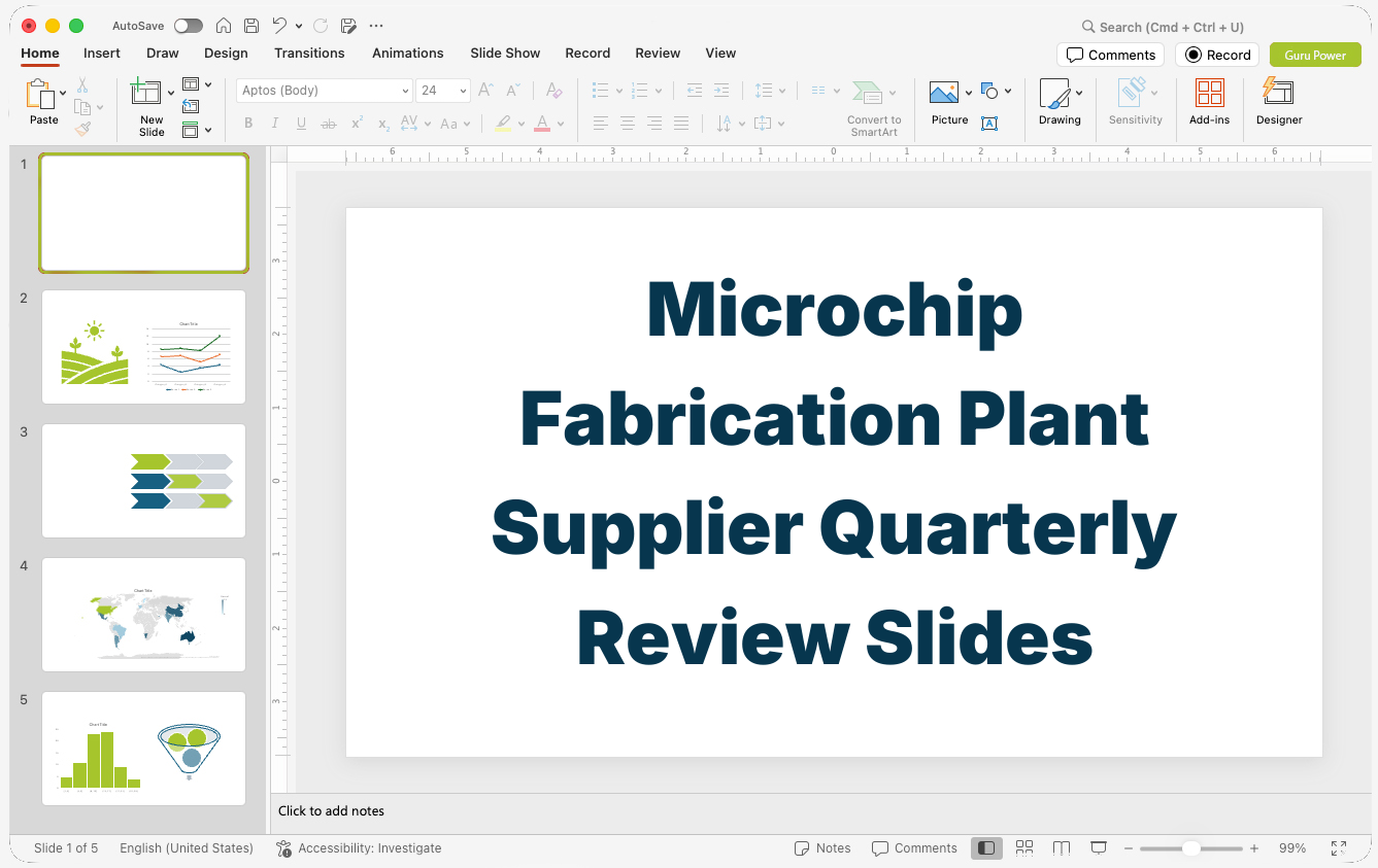
Microchip Fabrication Plant Supplier Quarterly Review Slides
Primary Audience: Silicon Wafers and Gas Delivery Vendors.
Purpose: Enforce vendor SLA compliance and defect reduction targets.
Description: These Slides review incoming material purity metrics, delivery reliability, and yield impact caused by substrate defects at the Microchip Fabrication Plant. The presentation compares vendor performance against baseline contractual commitments. Procurement teams leverage this structure to negotiate quality improvement plans.
Your PowerPoint, Google Slide and KeyNote Strategy, Story and Design Professionals
Presentation Gurus delivers end-to-end design, narrative structure, and brand consistency tailored for semiconductor manufacturing leadership. Our team transforms dense technical schematics and financial models into compelling visual presentations. Every presentation project undergoes strict quality controls to ensure structural clarity and corporate design alignment. Work with a design partner that understands high-tech manufacturing capital cycles. Contact Presentation Gurus today to review your upcoming presentation requirements and schedule an initial consultation.
Ready ToGet Started?
Presentation Gurus is open.
Give us a call.
We actually answer the phone.
Questions & Answers
Semiconductor Fabrication Plants Presentations FAQs
Does our industry need a Presentation or a Pitch Deck?
The terms are frequently used interchangeably, but they serve different strategic purposes. A pitch deck is a highly visual, persuasive tool designed to secure a strategic commitment or investment. A standard presentation is an informative, detailed document structured to align stakeholders and share data.
What does Semiconductor Fabrication Plants Presentations presentation design cost?
Pricing is simple and clear. A basic slide design or redesign begins at $49 per slide. Premium presentation design, which includes copywriting and basic storytelling, starts at $79 per slide. Custom presentations involving strategy, copywriting and custom graphics are quoted based on your specifications. See complete pricing details here.
How does the collaboration process work?
Everything happens online. Every meeting is a Microsoft Teams call or similar virtual environment where we can share desktops and information in real time. Revision meetings and discovery calls are always scheduled in the morning, so by noon we can begin work on tasks for the next revision meeting.
Do you design templates that internal chip foundry teams can edit later?
Yes. We deliver fully editable PowerPoint files with custom master slide layouts, standardized typography, and scalable vector icon libraries tailored for ongoing internal operational updates.
How long does it take to get a presentation designed?
If your team needs a complete presentation by 9:00 AM the next day, we can meet that deadline. Most projects take 10 – 15 days, providing we have all the information. Pricing is also based on slide complexity and speed — a basic slide deck with a 15-day delivery costs much less than a premium slide deck delivered the next morning.
We have sensitive business information. Can you work under an NDA?
Virtually all of our client work is done under an NDA. We have a basic NDA included with our presentation work order, plus an enhanced, expanded non-disclosure agreement available whenever a project calls for it.
What is the typical turnaround time for a fab capital expenditure slide deck?
Standard turnarounds for complex business presentations range from 5 to 10 business days depending on slide count and custom visual asset requirements. Accelerated timelines are available for time-sensitive funding applications or earnings reports.
Can you convert complex wafer yield data into executive PowerPoint slides?
Yes. We translate dense engineering metrics, tool utilization charts, and yield defect data into clear visual charts suited for executive board members and institutional investors.
Will our team receive the fully editable source file?
Yes. Unlike graphic designers who deliver flat PDFs or JPEGs, Presentation Gurus delivers the native, fully editable presentation file (.pptx, .key, etc.) so your team can make last-minute text edits on the fly, or update the presentation later as details change.
How do you handle technical confidentiality during presentation design for semiconductor facilities?
Presentation Gurus executes mutual Non-Disclosure Agreements (NDAs) prior to receiving any project materials. All data handling and slide design workflows adhere to strict corporate security standards to protect proprietary process node and yield metrics.
Presentation Gurus' research identifies 12 locations with active Semiconductor Fabrication Plants operations, including Phoenix, AZ, Austin, TX, and Hillsboro, OR.
Capital projects and technical cleanrooms define the modern semiconductor footprint across the United States. In Phoenix, AZ, multi-billion dollar construction projects from TSMC and Intel anchor substantial growth, with nearby Chandler, AZ operating high-volume manufacturing lines at Intel’s Ocotillo campus. Supporting supplier networks and specialized labor operate right alongside in Maricopa, AZ, underscoring how Arizona has made advanced chip foundries a pillar of its industrial economy.
The momentum continues throughout the Pacific Northwest and Mountain West. In Hillsboro, OR, Intel operates its Gordon Moore Park campus and leads advanced technology development fabs. That enterprise makes Intel the largest private employer in Washington County, reinforcing the importance of Oregon and its Sunset Corridor. Meanwhile, Boise, ID serves as the global headquarters and primary memory research and manufacturing site for Micron Technology. Down in Lehi, UT, Texas Instruments operates a dedicated 300mm wafer fabrication plant acquired from Micron.
Texas also remains a core hub for wafer fabrication and logistics. In Austin, TX, Samsung Electronics and Texas Instruments maintain large-scale manufacturing facilities. Up in Richardson, TX, the historic Telecom Corridor supports active analog chip production lines for Texas Instruments, while Plano, TX provides corporate management and supply chain coordination for regional foundries.
Major expansion extends into the Midwest and East Coast as well. A massive multi-billion dollar mega-fab site is underway in Columbus, OH across Licking County. In Upstate New York, Utica, NY hosts Wolfspeed’s Marcy Nanocenter Silicon Carbide wafer facility, and nearby Syracuse, NY connects to Micron’s planned mega-fab memory manufacturing complex in Clay.
The scale of these facilities ties directly into neighboring industrial supply chains. Presentation Gurus partners with teams across these production ecosystems through dedicated presentation design services. The operational complexity of microelectronics frequently intersects with Industrial Automation & Robotics, Automotive Manufacturing & Assembly, and Electric Vehicle (EV) & Battery Manufacturing. Similar infrastructure demands exist in Aerospace & Defense Contractors, Heavy Machinery & Industrial Equipment, Building Materials Manufacturing, Packaging & Paper Product Manufacturing, and Food & Beverage Processing Facilities, where clear technical reporting and stakeholder alignment remain critical.
Semiconductor Fabrication Plants Presentations By the Numbers
- The global semiconductor market was valued at USD 668.27 billion in 2025 and is projected to reach USD 711.57 billion in 2026. (Global Semiconductor Market Size, Share & Growth, 2034)
- The CHIPS and Science Act allocated $52.7 billion in total federal funding to strengthen domestic semiconductor research, development, and manufacturing. (CHIPS and Science Act – Wikipedia)